Building Computing Machines from Ground Up: Basic CPU
revision 1.1.0
In this post I will discuss CPU: what it is in its simplest form and what is required to build one. I will illustrate the post with circuits modelled in Logisim.
CPU Demystified
When trying to understand CPUs it is crucial to remember that internally they consist of a multitude of much simpler elements: registers, counters, basic logic gates. Each of these subunits is quite unsophisticated, but operating together in proper order they create complex behaviour of a CPU. The work of CPU is a carefully orchestrated sequence of actions of the subunits. Therefore the task of designing a CPU breaks down to figuring out which subunits are necessary to fulfil higher-level contracts and how they should interact, in which sequence and with whom.
Consider a counter. On a figure below it is shown as it is seen by a user of Logisim.
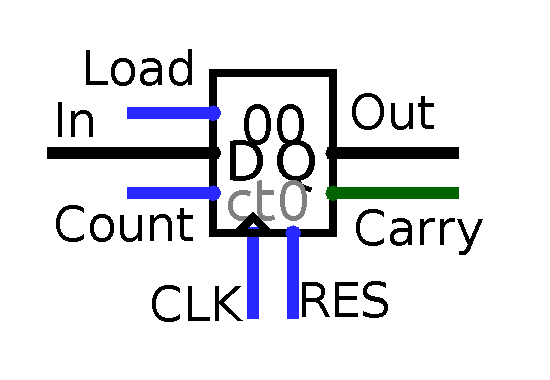
A counter. 'In' -- 8-bit wide input; 'Out' -- 8-bit wide output; 'Load' and 'Count' -- single bit control inputs; 'CLK' -- clock input; 'RES' -- asynchronous reset input.
A moderately complex circuit which could store, load, increment or decrement binary values. Without any external stimulus a counter just stores whatever happens to be inside it as long as power is present, with output set to stored value. When a clock pulse arrives the counter performs one of four actions depending on which logic levels are present on its control inputs. Options available are presented in a table below
LOAD    COUNT      ACTION ON CLOCK
-------------------------------------------
  1       0      Load value from data input
  1       1      Decrement value
  0       1      Increment value
  0       0      Do nothing
Reset input is asynchronous: whenever a pulse arrives it resets value to zero.
Now consider the following scenario: some value present on input must be incremented. I believe it is rather obvious that it could be done by first loading the value into the counter, then incrementing it. To load a value one must set ‘In’ bus to it, set ‘LOAD’ to high, ‘COUNT’ to low and then issue a clock pulse. To increment the value ‘LOAD” must be set to low, ‘COUNT’ to high and a clock pulse must be applied. Note that each of the four steps above could be represented with constant levels on corresponding inputs:
          LOAD     COUNT    CLOCK
---------------------------------
Step 1      1        0        0
Step 2      1        0        1
Step 3      0        1        0
Step 4      0        1        1
If only a way existed for creating such tables in hardware! Then proper level changes would have happened when stepping through rows. Good news are that such tables are not only possible, but are quite trivial to implement. The values themselves could be as simple as resistors pulling to either high or low level, selection between steps could be achieved with multiplexers:
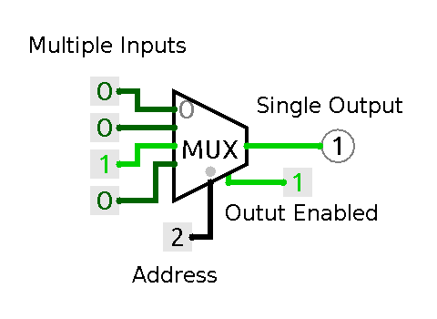
A multiplexer. 'Address' -- 2-bit wide bus, 'Output enabled' -- allows a signal to propagate from one of inputs to output when set to high.
A multiplexer connects one of its inputs to its output depending on input address value. Thus the only thing left is to provide means to actually select an input. Fortunately we already have counters at our disposition, so we can use one four-bit counter to count pulses from some source and drive a multiplexer:
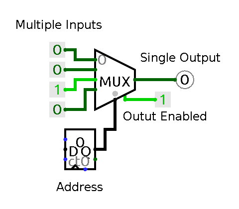
A multiplexer with line address provided by a counter.
Putting everything together it is easy to build a circuit that looks and operates like the one below:
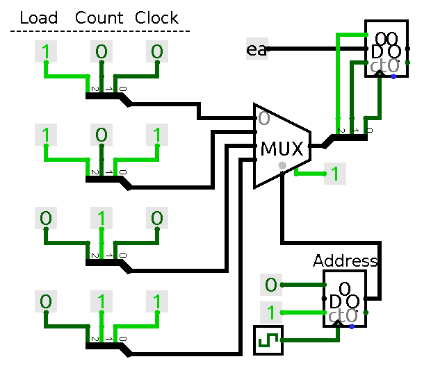
A circuit that performs 'Load and Increment' operation. Each step is encoded with three constants 'Load', 'Count' and 'Clock' which determine logic levels on corresponding input of a counter. Constant groups are connected via 3-bit buses to a multiplexer which switches between them depending on step number provided by step counter.
A counter counts pulses producing sequential addresses for multiplexer to step through control table. Multiplexer in turn switches between input values. Note, that Logisim allows to switch an entire bus with a single multiplexer which I did in this example. In real world one would need to use several multiplexers together to achieve the same results.
This circuit does not perform anything useful yet, but it illustrates how one can orchestrate complex behaviour of different components. Consider, for example, two such counters, one of which provides an input for another. It is easy to imagine a table that would copy a value from one to another. What could be the use for such a setup, a careful reader might wonder? Well, name the first counter A, the second counter B and get a free mov A, B implementation.
Back to the load and increment (LAI) circuit. What if one needs to not only increment, but possibly decrement a value loaded into the counter (i.e. implement LAD)? Certainly a table for load and decrement would come in handy:
          LOAD    COUNT    CLOCK
--------------------------------
Step 1      1       0        0
Step 2      1       0        1
Step 3      1       1        0
Step 4      1       1        1
This table could be implemented in exactly the same way as the previous one. Now to be able to switch between two functions some device is needed that somehow selects which table to use. For example, one could decide to switch control signals for the counter with yet another multiplexer with one bit address. Address input of this second multiplexer could be fed with a code representing either LAI or LAD action. The action to be performed could be selected with a simple mechanical switch or a constant in the case of Logisim circuit:
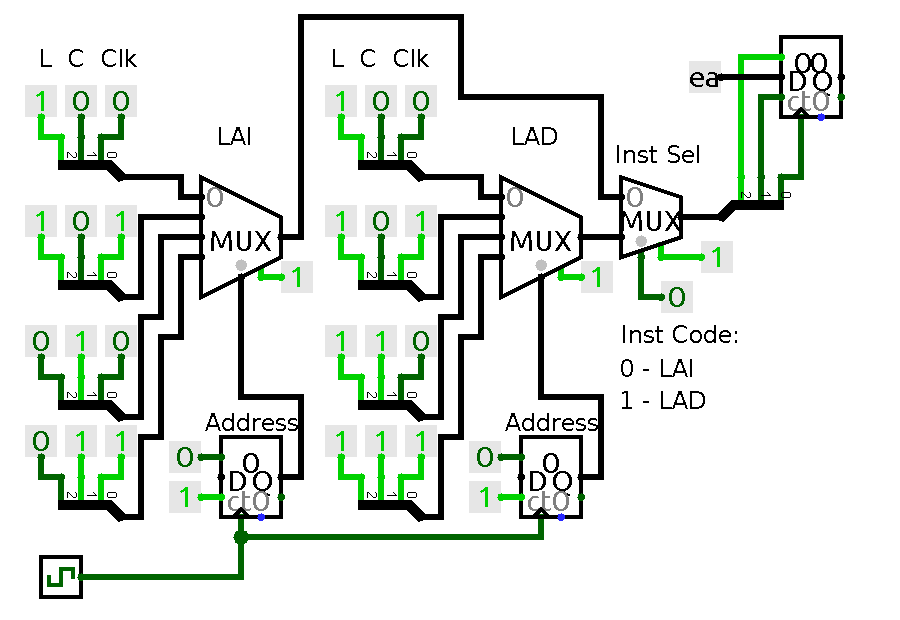
LAI/LAD basic circuit. Multiplexer tagged with 'LAI' governs Load and Increment instruction, multiplexer tagged with 'LAD' governs Load and Decrement. 'Inst Sel' multiplexer selects which of control tables to use to drive the counter.
What if several LAI or LAD actions have to be implemented in sequence? One option is to manually toggle operation control switch when needed, the other one is to use one more table to store the sequence of operations to be performed. Consider this – an addition counter, let us call it ‘Program Counter’, points to position in this sequence table which is again implemented as a multiplexer switching constant values. Program counter gets advanced each time any of operations has finished. In general this could be achieved by adding an extra column to control tables of operations, which would reset operation counter and increment program counter. Also it might be necessary to block operation counters for all operations except the current one since different operations could consist of different number of steps and allowing all counters to increment would result in them being in random state at the start of their operation execution. Alternatively one could consider resetting all operation counters prior to operation execution. In the case of LAI/LAD, however, it is possible to shortcut a little: first of all, both operations have the same length, so operation counters can safely run in parallel without causing inconsistencies, and second both operations require four steps to be performed, which allows to use simple counters which naturally reset to zero when reaching the last step. Counter overflow also generates carry pulse which could be used to advance program counter. Resulting circuit is shown below:
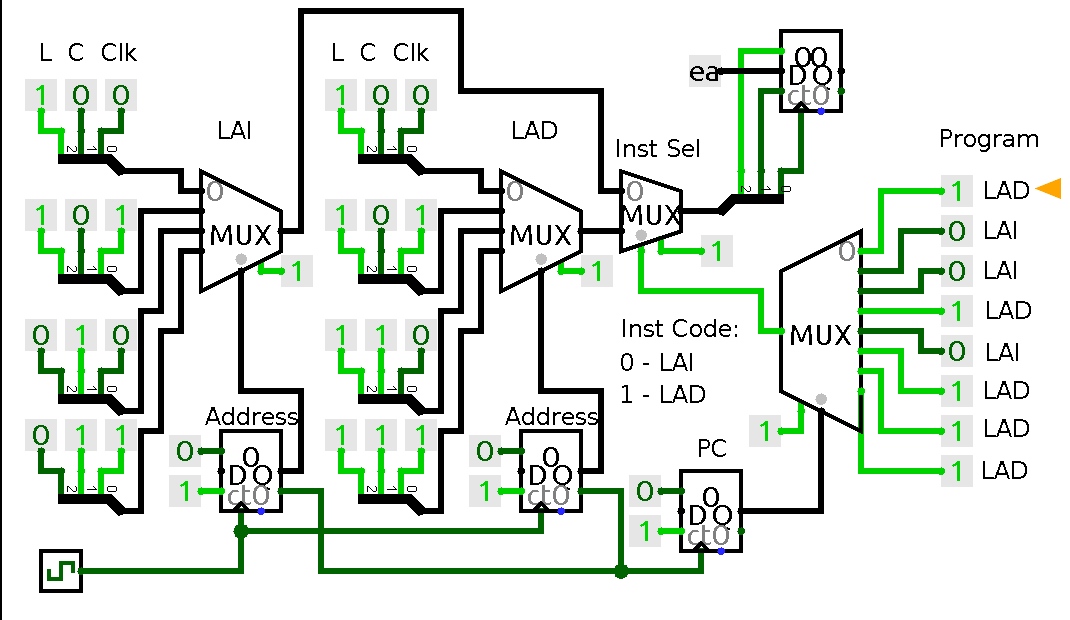
LAI/LAD circuit equipped with a program counter (PC) runs a program.
The circuit above could be optimized since most of control signals remain the same for both instructions and thus could be produced by one table, but doing so will needlessly overcomplicate the example so I will not do that now.
Actually this is basically all one needs to build a CPU: just throw in control tables for all individual instructions, add some switching logic that selects proper table basing on current instruction value and possibly the state of CPU – both flags and values held in registers could affect selection, and that’s it. The only problem with this approach is that it is rather tedious and error-prone. If designed without proper care addition of new instructions or modification of existing ones could affect large parts of circuit and introduce rather unpleasant bugs. In short, this approach does not scale easily.
Fortunately this is not the only option available. The other option is to use read-only memory with some additional components to implement control unit.
ROM-based Control Unit
Instead of wiring multiple multiplexers one could use read-only memory.
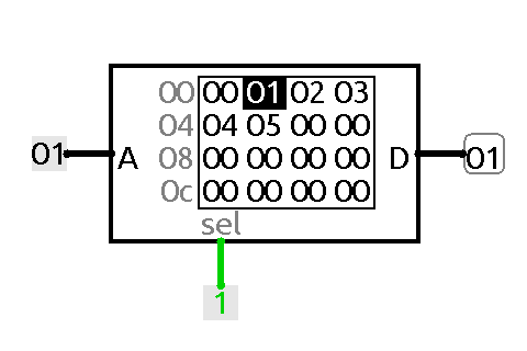
A ROM. 'A' -- address input; 'D' -- data output; 'Sel' -- chip select, supposed to shut memory off the circuit with tri-state buffer when chip is not used.
Memory implementation choices are the topic of a separate post, so for now let us do some wishful thinking and pretend that we already have ROMs: devices that map addresses to values. In the context of a control unit for a CPU ‘address’ is somewhat misleading term since we are interested in mapping between a combination of code of instruction to be carried out, number of step inside that particular instruction, possibly some internal state flags (for instance consider control of conditional jumps) and a vector describing both current state of all control pins of all subelements and next step to be taken.
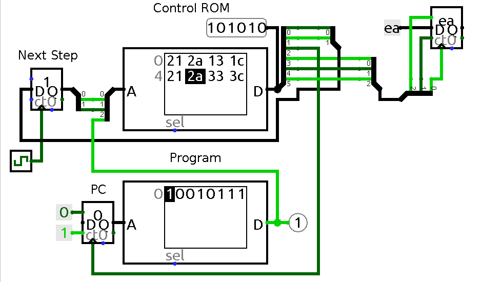
A figure below shows how a ROM could be wired to be used as control unit:
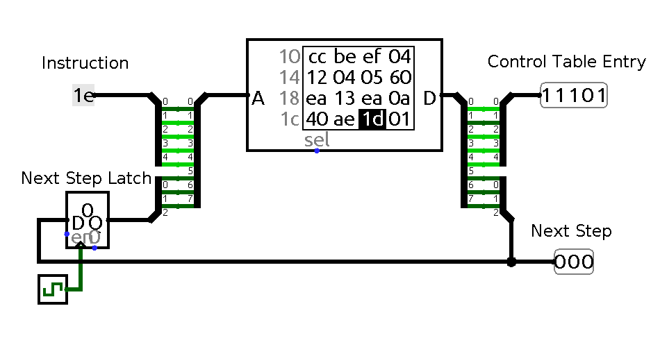
Basic ROM-based control unit. Here address in ROM is obtained from current instruction and value stored in 'Next Step' register. Location in ROM defined by this combination (Control Table Entry) consists of a control vector defining states of all control inputs of all subunits for this step and next step to be taken.
A step register holds current step, switching to the next step happens on clock. Clock pulse makes step register latch the next step code. That in turn transform the next step into current one and causes ROM to change its output accordingly. Now to build a control unit one has to populate a ROM with proper values. Below is an example of a control table implementing LAI/LAD instructions:
             ADDRESS            STORED VALUE
          +-----------+   +----------------------+
MNEMONIC  CODE     STEP   STATE VECTOR   NEXT STEP   -->   ADDR    VALUE
------------------------------------------------------------------------
LAI        0        00        1000          01              00      x21
           0        01        1010          10              01      x2a
           0        10        0100          11              02      x13
           0        11        0111          00              03      x1c

LAD        1        00        1000          01              04      x21
           1        01        1010          10              05      x2a
           1        10        1100          11              06      x33
           1        11        1111          00              07      x3c
------------------------------------------------------------------------
STATE VECTOR = [LOAD, COUNT, CLK, PCCLK]
Note extra PC clock added to the state vector which is needed to step over to the next instruction.
Built around this ROM-based control unit LAI/LAD machine will look like this:
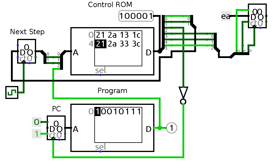
LAI/LAD built with ROM control unit. ROM used for the control unit has 3-bit wide address bus and 6-bit data bus. Program ROM has 3-bit wide address bus as well and 1-bit data bus which is enough for simple tests.
Note that “program” is stored in a ROM as well. Also note an inverter in the PC clock line: by default a counter in Logisim updates its state on the rising edge of clock pulse which is a little undesirable here, since it would cause PC increment and stepping out of a command before it is finished. Thus a counter must either be explicitly configured to use falling edge or a negating element could be used to swap edges.
While being rather wasteful gate-wise this implementation of control unit is very easy to understand and reproduce. More importantly it is exceptionally easy to extend, all one needs to do is to populate corresponding spaces in ROM. And in case of running out of space in one ROM one could easily add more ROMs. The same holds true also for the state vector’s size: if you are not satisfied with data port width of your ROM just connect several of them in parallel. Also I personally find it good that such control unit could be designed and debugged with just pen and paper in the most straightforward manner possible. Of course having an automated tool for filling such tables reduces the strain, but I like to have a back-up low tech option available. Another interesting option that could come in handy for control table debugging is RAM-based control unit which can speed-up testing and debugging real hardware. Moreover, such control units allow to add instructions gradually to already working systems, or even modify them in run time which could be a source of endless fun and occasionally of bugs.
Afterword
The design above touches lightly on the topic of building a CPU. Moreover, it is deliberately crude and unoptimized. Yet I hope it turned to be very straightforward and easy to understand. I have deliberately left out lots of topics like control ROM space optimization which could be achieved by compressing state vector and using auxiliary circuitry to decode it, embedding control sequences into instruction codes themselves or removing most of the ROM altogether and relying instead on multiphase clock and careful instruction design. While capable of producing much more compact designs I believe these techniques obscure the basics, and having good grasp of basic designs, even crude ones, is essential for being able to come up with optimisations when such need arises.
Another possibly surprising decision is not to discuss arithmetic-logic units. I find ALUs simultaneously trivial enough and well-described in multiple sources and complicated enough to distract from important question of subcomponent orchestration. Moreover, it is perfectly possible to build a CPU completely lacking distinct ALU and it would be as complete as any one with it (consider, for example, a BrainFuck computer). Thus I decided to discuss them later in a separate post.
Updates
00 Original version of this blog post contained a slightly different animation of a LAI/LAD ROM-based circuit. It lacked inverter on PC clock line which resulted in harmless (for this design), but rather untidy jumps at the end of some command execution. It looked like this:
PC jumps over the last step of current to a different command.
As Settis has accurately noted this behavior while not being exactly wrong is rather confusing, so I updated the post with improved circuit animation.
Another kudos goes to Yar for pointing out multiple inconsistencies in the original post and providing suggestions on improvement.
Also following the feedback I am adding a repository with Logisim projects and images used in this series so everyone could experiment with them.