Building Computing Machines from Ground Up: BrainF--k Interpreter
revision 0.7.3
In this post I will build upon a design of simple programmable counters and implement a primitive BrainF–k machine.
BrainF–k Revisited
BrainF–k is a minimalistic programming language that is supposed to be interpreted by a BrainF–k machine. This machine consists of two tapes, one (unlimited) for program, another looped one for data. Data tape contains 2^15 locations or cells each of which can store an 8-bit value. A head can move along data tape, increment or decrement current value or reading or writing value from or to user. Head action is determined by current value of program tape. After current instruction is processed head steps to an adjacent instruction written on program tape.
There are just eight possible instructions, which is four more than needed to be Turing complete1: since tape and cell values are finite and can flip over there is no real need for decrements. Two extra instructions (for user i/o) are added for convenience, in principle they are not needed as well since input can be preset before starting the machine and output collected if it ever stops. Below is a reference table of BrainF–k commands:
COMMAND  No   EFFECT
-------------------------------------------------------------------------------
   +      0   Increment value in current head position;
   -      1   decrement value in current head position;
   >      2   move head right (i.e. increment head position);
   <      3   move head left (i.e. decrement head position);
   .      4   output current cell value;
   ,      5   input into current cell;
   [      6   do nothing if current value is nonzero, fast-forward to command
              after matching ] otherwise;
   ]      7   do nothing if current value is zero, go back to command after
              matching [ otherwise.
The machine is extremely simple and an emulator could be trivially implemented in any non-esoteric programming language in a matter of minutes. Having refreshed what BrainF–k is let us dive into implementation of the machine in hardware. But before that
A word on tapes
When talking about Turing tar pits a term “tape” is frequently used. This word bears a distinct sound of age long gone and can confuse, but in reality it merely states the fact that memory device used in a machine is sequential. Thus there is no need to use real tape for building a BrainF–k machine, anything that allows sequential access to data stored inside will do. For example RAM chip for which address is generated by a counter can serve as an example of tape emulating device: the only way to access any given location in memory is to count up or down towards it from current one. A possible circuit is presented on the image below:
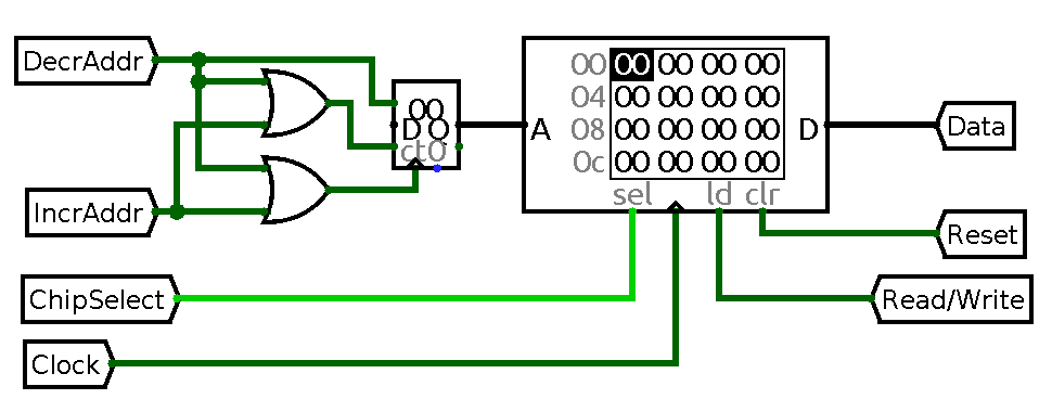
Sequential memory unit made out of ordinary RAM and a counter. Transition to high on IncrAddr and DecAddr inputs increments or decrements current address respectively. Data is a bus shared betweeen imput and output, Read/Write toggles chip operation mode between reading data from it and writing data to it. Reset asynchronously clears memory, ChipSelect enables or disables component, pulse on Clock input writes value to memory.
I have not described RAM chips yet, but Logisim implemtation is quite similar to ROM with the difference of extra inputs allowing to write data to addresses present on address input. Conceptually it would probably be right to use circuit similar to described above as a tape emulator and some other circuitry to emulate head. In fact BrainF–k machine that I designed first historically did exactly this. Such approach is also closer to more traditional computers where one can separate CPU from data and program memory. However I will not follow this route because on one hand it would further break my commitment to medium scale ICs (which I still have to unbreak by replacing control ROMs with something less integrated), on the other hand even when RAM is made from scratch the solution does not scale down well. RAM units are not really complex, however they are extremely repetituous and labor-intensive: hundreds or even thousands of identical subuntis must be produced to assemble RAM and it does not make much sense to build RAMs to capacity of several bytes. Any possible gain of proper RAM unit would be negated at such capacities and in the end will require additional effort to bring in more such elements.
Instead I decided to design BrainfF–k machine around memory device consisting of indvidual cells, each of which is responsible for decoding address in memory and acting upon that. Such decision significantly increases component count and price of a final machine, but at the same time gives several advantages. First of all, if each cell is independent one can add as many cells to minimal working solution as she sees fit: eight cells would work as good as twenty or one thousand twenty five. When a need for more memory arises more cells could be added seamlessly provided that address bus capacity is not exhausted. For example BrainF–k machine could be demonstrated to operate properly with three cells avaliable on tape, but more complex programs like fixed point arithmetics computations or equations solvers would require several times more cells while emulators of other computing systems would happily claim as much memory as a user could afford. Another advantage lies in ability to visualise cell contents and behavior. Adding several LEDs to each cell allows one to easily monitor its operation, provides very straightforward debugging tool and even allows one to create makeshift output device with little overhead.
Consider once again a counter described in the previous post. It can load and store data. Several such counters could be used together to store more than one value. A multiplexer could be used to select which counter to use basing on a value in another counter. This departs from the original plan of address self-decoding, but I believe that it is fine for demonstration purposes and address-aware cells could be introduced separately as a drop-in replacement. The behavior described so far could be much easier implemented with plain registers, but counters allow for one extra shortcut: I don’t need to design a separate block for arithmetics any more, since each memory cell is capable of incrementing and decrementing! All I have to do is to come up with a bus that will route all necessary signals properly.
The resulting “tape” then will look like this:
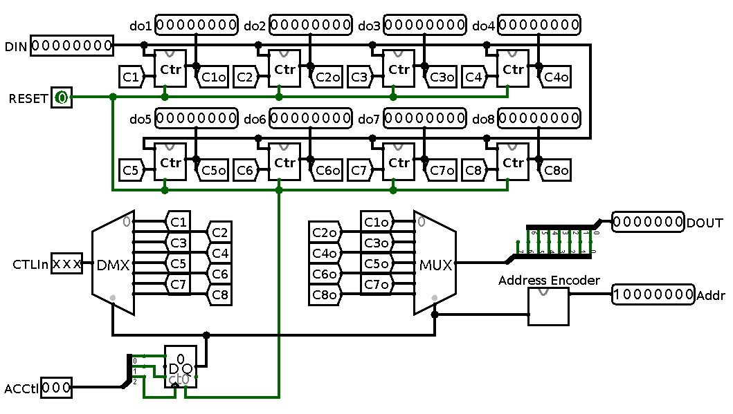
Sequential memory unit made from discrete counters. Eight counters are connected to demultiplexed control bus CTLIn, their outputs multiplexed and outputed to DOUT after being trimmed to 7 bit width. Data could be written to current cell through DIN port, cell selection is done by a counter driven by ACCtl input. For demonstration purpose address is encoded as 8 bit value and output through Addr port. Each counters output is connected to a separate output port to support visualisation.
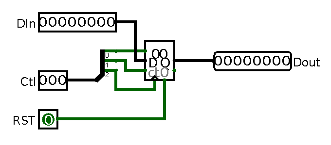
An individual counter wiring for sequential memory unit.
This approach while very handy for BrainF–k machine blurs the border between CPU and memory as they are present in more practical computers. That said a BrainF–k machine as described below could be easily modified to use RAM chip and distinctive head – a single counter could perform increments and decrements of values, provided that control ROM contains descriptions of steps necessary to load values from memory and to store them back.
Note that here I heavily use Logisim tunnels, entitites that share state with peers of the same name. This feature is extremely handy because circuits tend to become a mess otherwise. Individual counters and necessary wiring is hidden in subcircuits. Also here I cut several more corners by using multiplexers to route control signals to cell selected via address input and to collect its output. In real world it will be rather hard to build a multiplexer that switches a bus between multiple addresses, moreover such design would be very unflexible. This problem could be solved by connecting each cell’s control inputs to the same source through two input AND gate with second input fed by cell’s address detector. Outputs can be bundled together in the same way with each individual output line ANDed with address detector output and then by performing OR between all same lines of all cells. Alternatively a tri-state buffer (a buffer which effectively shuts output off by switching to third, high-impedance state) could be used instead of logic gates. Note, however, that both solutions have drawbacks. Tri-state buffers are expensive and could be not available in component base of choice, and multi-input OR gates built by cascading regular two to four input gates introduce huge propagation delays: it takes time for each individual cell to change its state according to input. Connecting them in series effectvely multiplies propagation delay of individual cell by the number of stages. Consider typical propagation time of a CMOS two input OR gate of about 60 ns. With sixty three stages it will take about 3.8 us for output to stabilize which translates to maximum feasible clock frequency of about 250 kHz. 255 stages would cap frequency at about 60 kHz. This problem could be mitigated by building custom multi-input OR gate, but this is a topic for a different discussion.
The memory unit shown above exposes 8-bit DIN bus for uploading data to current cell, 3-bit CTLin bus for control signals to drive individual cells, 3-bit ACCtl bus to drive address counter and a 1-bit reset input. It provides output DOUT for reading current value trimmed to seven bit, but more of that later. Note that I decided to make address counter part of memory unit. I did it for demonstration purpose only. The way it is done now it will make stacking such memory units a much harder task than it should be.
Below is an image of a sequential memory unit connected to a LED matrix for the purpose of memory state visualisation:
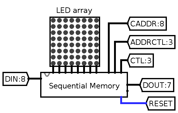
Sequential memory unit connected to LED array to visualize memory contents. DIN -- data input, CADDR -- current address output, ADDRCTL -- address counter controls, CTL -- memory cell control inputs, DOUT -- data output, RESET -- reset input. A number after colon denotes port width.
As for program tape regular ROM with a program counter will do the trick.
Having discussed how tapes could be approached let us move towards the design itself.
Fist half of commands
I will start with first four commands from the table above. They all are very
similar and actually quite familiar since they increment or decrement a single
value, data value in case of + and - and address in case of > and
<. I will use the same technique as before: use a table stored in ROM in
conjunction with a register to drive other elements.
To populate the table let us first enumerate all possible commands in the language. I suggest following enumeration from the table above. I believe now it should be pretty clear that control table will be almost identical to the one seen in previous post since the logic and the sequence of steps are pretty much the same. Now since there are several counters in the circuit I introduce two CTRSEL lines which will help me to route control signals to proper counters.
             ADDRESS            STORED VALUE
          +-----------+   +----------------------+
Command   CODE     STEP   STATE VECTOR   NEXT STEP   -->   ADDR    VALUE
-------------------------------------------------------------------------------
 +         000      00        010 00        01             0x0      0x21
           000      01        011 00        10             0x1      0x32
           000      10        010 11        11             0x2      0x2f
           000      11        011 11        00             0x3      0x3c

 -         001      00        110 00        01             0x4      0x61
           001      01        111 00        10             0x5      0x72
           001      10        010 11        11             0x6      0x2f
           001      11        011 11        00             0x7      0x3c

 >         010      00        010 01        01             0x8      0x25
           010      01        011 01        10             0x9      0x36
           010      10        010 11        11             0xa      0x2f
           010      11        011 11        00             0xb      0x3c

 <         011      00        110 01        01             0xc      0x65
           011      01        111 01        10             0xd      0x76
           011      10        010 11        11             0xe      0x2f
           011      11        011 11        00             0xf      0x3c
-------------------------------------------------------------------------------
STATE VECTOR = [LOAD, COUNT, CLK, CTRSEL:2]
CTRSEL:
00 -- current cell counter   01 -- address counter   11 -- program counter
Since all commands are basically identical let’s discuss the first one. It consists of four steps. First two steps increment counter 0b00 which is current memory cell: load for counter 0b00 is set high, then while it is sill high clock pulse is sent to counter 0b00. Second two steps are identical, but are performed for counter 0b11 which is program counter.
An animation of a circuit that can run programs consisting solely of these four commands is shown below
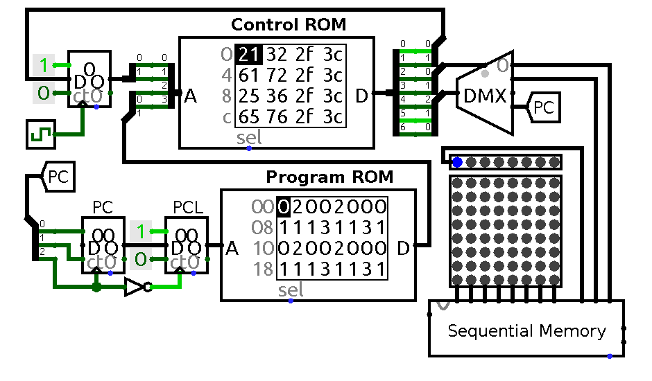
A circuit that implements first four commands. PCL -- PC latch, blue LEDs indicate current memory location.
Control ROM data line has the same structure as state vector in control table footer. The program which is running on the animation above is the following:
+>++>+++---<--<-
Note that sequential memory unit also outputs its address for demonstration purpose. Also note that in this circuit PC connected to program ROM through additional register clocked by falling edge of PC clock. This is done to prevent final step jumps: simple inverter is not enough in this case because control signals are not static any more and change values simultaneously with clock. That is the reason to introduce one extra latch to hold current address until it is not needed any more. Also it might be tempting to reduce the number of steps needed to modify counter contents to just one, but in practice that could lead to erroneous counter updates when transitioning from one step to another so I decided to play it safe and keep separate step for control setup and clock update for now.
So far so good! One half of the commands are dealt with. Now let us finish the task and add missing commands, they can’t be that different, can they?
Adding I/O
The next two commands in the table are . for output and , for input. The
main problem with output is the need for a proper device to which data will be
written. Again we see an example of a device which requires more patience than
ingenuity, since any electronic output device could be reduced to an array of
memory elements with some auxiliary logic to process line feed, carriage return
and other control symbols. A rudimentary terminal could be rather easily built
with enormous amount of shift registers, a ROM with symbol table, and some
counters with little control logic. I will, however, postpone this
demonstration and will use terminal emulator provided by Logisim. It has quite
simple interface – one 7-bit data input for ASCII values and clock input which
actually puts a symbol present on data input on screen.
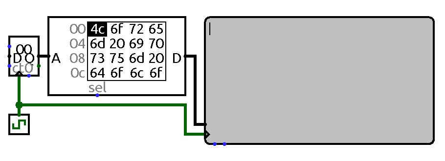
ROM contents is fed to a display. Memory data output is sent directly to display data input, the same clock pulse is used to both cycle through memory and to update display.
Thus to output cell contents to a terminal this data must first be put on terminal data input, then a terminal clock pulse should be issued. First part comes for free – cell contents is always present on sequential memory output. It only has to be trimmed to fit ASCII width. The pulse could be done the usual way. Thus previous control table could be extended with the following one:
             ADDRESS            STORED VALUE
          +-----------+   +----------------------+
Command   CODE     STEP   STATE VECTOR   NEXT STEP   -->   ADDR    VALUE
-------------------------------------------------------------------------------
 .         100      00       0000 10        01             0x10    0x09
           100      01       1000 10        10             0x11    0x8a
           100      10       0010 11        11             0x12    0x2f
           100      11       0011 11        00             0x13    0x3c
-------------------------------------------------------------------------------
STATE VECTOR = [TERMCLK, LOAD, COUNT, CLK, CTRSEL:2]
CTRSEL:
10 -- no counter selected   11 -- program counter
Not much to discuss here – a new control line is added to drive clock input of terminal device, its change to high is padded in the table (step 0b00) to avoid spurious terminal updates.
Output was quite straightforward, even though it required a new complex device
to be used and I had to increase my backlog of promises by one more entry.
Input is a little more involved. Let us pause for a moment and consider what
does it mean to input data into machine. From perspective of a counter it means
that I must set proper values on control inputs and then generate clock pulse
when the data is available on data input. The last part poses a problem: this
data is provided by a user and even slowest machines will operate much faster
than the fastest of users could react to data input prompt and toggle switches
or press buttons. Thus the machine must stop doing anything until user finishes
entering data. This effectively means that machine must freeze mid-command.
That, in turn, means that after starting sequence for , machine must stop
reacting to clock input until user allows it to continue. It is tempting to
break clock line with some logic to achieve just this, but it is better not to
since it is an antipattern which won’t harm in this particular case, but has
great potential for elusive bugs in more complex designs. It is better to
prevent next step latch from operating by changing its control inputs states.
Indeed if constant value at load input is replaced by inverted output of a
one-bit latch then its operation is unchanged. Then we can asynchronously set
the latch which will result in next step latch stopping to react to clock
input. Providing a button which asynchronously resets the latch to the user
would allow the machine to continue operation after the user is done with
input.
Thus the sequence of steps should look like this: first stop the machine by blocking next command latch, then (when it gets unblocked by a user) set current cells controls to load value from input, issue clock pulse to current cell, then increment program counter. Resulting addition to control table will look like this:
             ADDRESS            STORED VALUE
          +-----------+   +----------------------+
Command   CODE     STEP   STATE VECTOR   NEXT STEP   -->   ADDR    VALUE
-------------------------------------------------------------------------------
 ,         101     000      10000 10       001             0x28    0x211
           101     001      00100 00       010             0x29    0x082
           101     010      00101 00       011             0x2a    0x0a3
           101     011      00010 11       100             0x2b    0x05c
           101     100      00011 11       000             0x2c    0x078
-------------------------------------------------------------------------------
STATE VECTOR = [HLT, TERMCLK, LOAD, COUNT, CLK, CTRSEL:2]
CTRSEL:
00 -- current cell counter   10 -- no counter selected   11 -- program counter
Note that one more control line, HLT, is added. Signal on HLT synchronously sets trigger which controls next step operation. Also I had to add another address line to account for the fact that now I need five steps to perform this operation. As a result the entire table must be amended to account for this change. In order not to clutter the text I put it here. Resulting circuit is presented on image below:
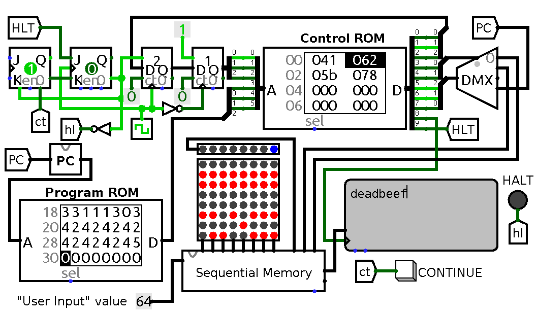
A circuit demonstrating I/O. HALT LED lights up when circuit is waiting for user input, CONTINUE button unsets J-K trigger which gets blocked by high level on HLT line.
The program it is running is quite straightforward:
,>,>,>,>,>,>,>,++<+<+<--<<---<+<.>.>.>.>.>.>.>.,
It reads eight values from input to eight neighbouring cells, modifies some values, prints results on a terminal and finally halts by starting to wait for more input. If all input values are 0x64 then after running the code combination deadbeef should appear on output device. On the schematic above I have hardwired input to be always equal to 0x64, but in real circuit one could use eight switches to produce desired result.
Now it is time for a word of caution. Wiring a button directly to asynchronous reset is definitely not the best idea. The button is human operated and when clock frequency is more than several hertz it becomes extremely easy to keep it pressed way after command processing is finished. Since asynchronuous reset is level-driven this will eventually lead to wrong values being read from input. Much better solution would be to make the button generate single pulse of fixed width per button press. However I did not come up with a clean way to do this in Logisim – it is possible to generate a pulse with an invertor and AND gate since propagation delays are taken into account to some extent, but I have not devised any straightforward way to debug it, so here is this warning instead. On the other hand in real circuit a 555 timer in standard single-pulse configuration should suffice.
Last two commands
Even after a cursory glance it becomes obvious that two final commands stand out from all previously seen. By definition each of them does not one, but two different things depending on condition which could be determined only in run time. When a cell that happens to be current when PC starts pointing to a bracket contains zero a sequence of actions differs from one when a cell is non-zero. Thus each command must have more than one entry in control table. This is somewhat new since all previous examples had only one and immediately poses a question: how exactly one could distinguish between different entries for a single command? Obviously runtime state should somehow be used to determine particular entry. And since entries start at different addresses an extra address line driven by run time state comes to resque. State of this line should be determined by the contents of current cell and could be easily generated by 8-NOR gate fed by cell output:
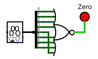
Zero flag implementation. Counter output is connected to 8-NOR gate. Counter holds value of 0 thus 8-NOR output is 1 which is indicated by LED labled 'Zero'.
Let us call this line Zero Flag. Now command code is extended by Zero Flag and proper step sequence is chosen depending on current cell state.
This immediately poses a question: what to do with other commands? It is impossible to introduce another address line and not to affect other commands. At the very least all locations would move, but in case of zero flag which became a part of address extra entries must be added to control table since it operates continuously and is present at every moment. Fortunately it does not affect execution of other commands so entries for them could be just copied to new locations in control ROM.
Another helpful property of the last two commands is their symmetry. You can
pick any one of them, invert all statements and you’ll have second command
description. Thus I’ll discuss only one command in details, second one could
be easily derived. For that I pick [.
The part when current cell is non-zero is trivial: do nothing which effectively means ‘do nothing, but remember to increment PC’. That easily translates into two entries in control table:
             ADDRESS            STORED VALUE
          +-----------+   +----------------------+
Command   CODE   Z  STEP   STATE VECTOR   NEXT STEP   -->   ADDR    VALUE
-------------------------------------------------------------------------------
 [         110   0  000      00010 11       001             0x60    0x59
           110   0  001      00011 11       000             0x61    0x78
-------------------------------------------------------------------------------
STATE VECTOR = [HLT, TERMCLK, LOAD, COUNT, CLK, CTRSEL:2]
Z -- zero flag, is 1 when contents is 0
CTRSEL:
11 -- program counter
Now let us look closer at the second part as it looks a bit tricky. The description says ‘fast forward to matching bracket’. Every word in this description is important. First of all, ‘fast forward’ means that address must be continuously incremented. No matter which command appears during this increment it must be skipped. Which in turn means that from now on each command must have two types of entries for it: one for regular operation, one for skipping any activity. This could be achieved by introducing another flag line driven by a trigger. Let us call this one ‘motion flag’. Since brackets are symmetrical I plan to reuse it later.
Second important phrase is ‘matching bracket’. Arguably the ability to nest
brackets define the power of the language, thus it is crucially important to
properly skip some brackets as well! Consider, for example, this snippet:
[>[-]-]. If when it is encountered address counter contains address of an
empty cell then everything inside the outer brackets must be ignored. How this
should be implemented? Note, that brackets in a correct program are balanced
i.e. the number of of opening and closing brackets match and first bracket in
any program is the opening one. Thus if one starts with an empty counter at
the beginning of a program, steps through it without executing commands and
increments the counter each time an open bracket appears and decrements it when
closing bracket is met, in the end this counter should contain zero as well.
This zero value will appear as soon as closing bracket were reached. The same
holds true for any subprogram inside a pair of brackets: a pair of brackets
can’t contain closing bracket for a bracket outside of it since it would cause
ambiguity. So if a subprogram starts with a bracket, we traverse it and update
counter as described and at some point see closing bracket simultaneously with
empty counter then this bracket is the matching one. This logic could be
implemented in hardware with yet another counter, let me call it bracket
counter, and a flag – matching bracket flag – to indicate that the counter is
zero. When matching bracket flag is 1 then the next bracket is matching and
motion flag must be toggled and thus normal operation should resume.
Unfortunately this requires yet another address line, but at least other
commands are not affected by it so no need to modify them, copying values is
enough. Note however, that other flags could in general affect what should be
done so don’t forget to copy responsibly.
Now let us look closely at [ one more time. Let us ask ourselves, have we
analysed interpreter’s behaviour in fullness? Let us imagine a slide over
program in search for matching bracket during which we meet [. Do we have
enough data to do the right thing? We have Motion Flag to tell us that we are
moving, we have zero flag which we don’t care about, finally we have matching
bracket flag to tell us whether we should stop. Looks almost good, but there is
this last instruction which was supposed to be absolutely symmetric and which I
was hoping to just generate automatically: it could initiate this slide as well
and that means that we can slide over [ in two cases, when searching for
matching ] and when searching for matching [. Which means that bracket
counter could be either incremented or decremented, depending on command which
has initiated this slide. Thus when updating PC during a slide we need one more
bit of data, namely movement direction to modify it properly. For that I will
introduce one more flag: direction flag. While the same result could have been
achieved with a latch and some basic logic without introducing an extra address
line I opted for an explicit flag since it makes it clearer what exactly is
going on. Finally it appears that [ is covered from all sides: regular
operation, movement and proper PC and flags update action depending on movement
direction.
Let me condense and revisit the discussion above before presenting you with a
full control table. After considering [ control ROM address bus got extra
four bits driven by flags: Zero, Motion, Bracket match and Direction.
Flags have the following meaning:
                                 0                             1
-------------------------------------------------------------------------------
[Z]ero               Current cell is not zero        Current cell is zero
[M]otion             Regular operation               Moving to find match
[B]racket match      Next bracket is not matching    Next bracket is matching
[D]irection          Moving forward                  Moving backwards
Depending on these flags [ is interpreted in the following ways:
- when a cell is non-zero and no motion is taking place then just increment the PC independently of remaining flags values2 ;
- when a cell is zero and no motion is happening toggle motion flag and increment PC;
- when moving and program pointer is moving forward increment bracket counter and PC no matter what are the values of zero flag or branch match (branch match will change anyway so no reason to care for its value now);
- when moving and moving backwards and bracket is not matched decrement bracket counter and decrement PC no matter what zero flag value is;
- when moving and moving backwards and bracket matches then toggle motion and direction flags and increment PC.
Reasoning about ] is basically the same so I won’t elaborate on it here.
Other commands are modified as follows:
- Original entry is kept for regular operation (i.e. Motion Flag equals to zero) and any other flags combinations;
- when moving and direction is forward just increment PC disregarding other flags’ values;
- when moving and moving backwards decrement PC.
Now we are ready to populate the final control table. To save space I will show only unique entries. I will denote that entry is the same for all values of a flag by replacing a value with X. Thus final table will look like this:
             ADDRESS                    STORED VALUE
          +--------------+       +-----------------------+
Command   CODE  ZMBD  STEP       STATE VECTOR    NEXT STEP  -->  ADDR  VALUE
-------------------------------------------------------------------------------
 +         000  X0XX   000       0000 010 000      001           ...  0x0081
           000  X0XX   001       0000 011 000      010           ...  0x00c2
           000  X0XX   010       0000 010 011      011           ...  0x009b
           000  X0XX   011       0000 011 011      000           ...  0x00d8

           000  X1X0   000       0000 010 011      001           ...  0x0099
           000  X1X0   001       0000 011 011      000           ...  0x00d8

           000  X1X1   000       0000 110 011      001           ...  0x0199
           000  X1X1   001       0000 111 011      000           ...  0x01d8


 -         001  X0XX   000       0000 110 000      001           ...  0x0181
           001  X0XX   001       0000 111 000      010           ...  0x01c2
           001  X0XX   010       0000 010 011      011           ...  0x009b
           001  X0XX   011       0000 011 011      000           ...  0x00d8

           001  X1X0   000       0000 010 011      001           ...  0x0099
           001  X1X0   001       0000 011 011      000           ...  0x00d8

           001  X1X1   000       0000 110 011      001           ...  0x0199
           001  X1X1   001       0000 111 011      000           ...  0x01d8


 >         010  X0XX   000       0000 010 001      001           ...  0x0089
           010  X0XX   001       0000 011 001      010           ...  0x00ca
           010  X0XX   010       0000 010 011      011           ...  0x009b
           010  X0XX   011       0000 011 011      000           ...  0x00d8

           010  X1X0   000       0000 010 011      001           ...  0x0099
           010  X1X0   001       0000 011 011      000           ...  0x00d8

           010  X1X1   000       0000 110 011      001           ...  0x0199
           010  X1X1   001       0000 111 011      000           ...  0x01d8


 <         011  X0XX   000       0000 110 001      001           ...  0x0189
           011  X0XX   001       0000 111 001      010           ...  0x01ca
           011  X0XX   010       0000 010 011      011           ...  0x009b
           011  X0XX   011       0000 011 011      000           ...  0x00d8

           011  X1X0   000       0000 010 011      001           ...  0x0099
           011  X1X0   001       0000 011 011      000           ...  0x00d8

           011  X1X1   000       0000 110 011      001           ...  0x0199
           011  X1X1   001       0000 111 011      000           ...  0x01d8

 .         100  X0XX   000       0000 000 010      001           ...  0x0011
           100  X0XX   001       0001 000 010      010           ...  0x0212
           100  X0XX   010       0000 010 011      011           ...  0x009b
           100  X0XX   011       0000 011 011      000           ...  0x00d8

           100  X1X0   000       0000 010 011      001           ...  0x0099
           100  X1X0   001       0000 011 011      000           ...  0x00d8

           100  X1X1   000       0000 110 011      001           ...  0x0199
           100  X1X1   001       0000 111 011      000           ...  0x01d8


 ,         101  X0XX   000       0010 000 010      001           ...  0x0411
           101  X0XX   001       0000 100 000      010           ...  0x0102
           101  X0XX   010       0000 101 000      011           ...  0x0143
           101  X0XX   011       0000 010 011      100           ...  0x009c
           101  X0XX   100       0000 011 011      000           ...  0x00d8

           101  X1X0   000       0000 010 011      001           ...  0x0099
           101  X1X0   001       0000 011 011      000           ...  0x00d8

           101  X1X1   000       0000 110 011      001           ...  0x0199
           101  X1X1   001       0000 111 011      000           ...  0x01d8


 [         110  00XX   000       0000 010 011      001           ...  0x0099
           110  00XX   001       0000 011 011      000           ...  0x00d8

           110  10XX   000       1000 010 011      001           ...  0x1099
           110  10XX   001       0000 011 011      000           ...  0x00d8

           110  X1X0   000       0000 010 100      001           ...  0x00a1
           110  X1X0   001       0000 011 100      010           ...  0x00e2
           110  X1X0   010       0000 010 011      011           ...  0x009b
           110  X1X0   011       0000 011 011      000           ...  0x00d8

           110  X101   000       0000 110 100      001           ...  0x01a1
           110  X101   001       0000 111 100      010           ...  0x01e2
           110  X101   010       0000 110 011      011           ...  0x019b
           110  X101   011       0000 111 011      000           ...  0x01d8

           110  X111   000       1100 000 010      001           ...  0x1811
           110  X111   001       0000 010 011      010           ...  0x009a
           110  X111   010       0000 011 011      000           ...  0x00d8


 ]         111  00XX   000       1100 110 011      001           ...  0x1999
           111  00XX   001       0000 111 011      000           ...  0x01d8

           111  10XX   000       0000 010 011      001           ...  0x0099
           111  10XX   001       0000 011 011      000           ...  0x00d8

           111  X1X1   000       0000 010 100      001           ...  0x00a1
           111  X1X1   001       0000 011 100      010           ...  0x00e2
           111  X1X1   010       0000 110 011      011           ...  0x019b
           111  X1X1   011       0000 111 011      000           ...  0x01d8

           111  X100   000       0000 110 100      001           ...  0x01a1
           111  X100   001       0000 111 100      010           ...  0x01e2
           111  X100   010       0000 010 011      011           ...  0x009b
           111  X100   011       0000 011 011      000           ...  0x00d8

           111  X110   000       1000 000 010      001           ...  0x1011
           111  X110   001       0000 010 011      010           ...  0x009a
           111  X110   010       0000 011 011      000           ...  0x00d8
-------------------------------------------------------------------------------
FLAGS = [Zero, Motion, Bracket match, Direction]
STATE VECTOR = [(TOGGLE_MOTION_FLAG, TOGGLE_PC_DIRECTION, HLT, TERMCLK),
                (LOAD, COUNT, CLK), CTRSEL:3]
CTRSEL:
000 -- current cell counter   001 -- address counter
010 -- no counter selected    011 -- program counter  100 -- bracket counter
I have not expanded address values since it would have taken too much screen space and put ellipses in their place. Final circuit is presented below:
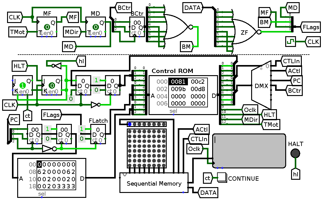
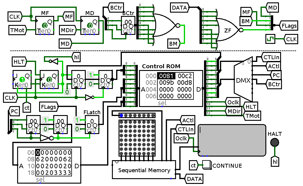
Final computer. Part of circuit below dashed line is essentially the same as for six commands with the exception of flag latch FLatch and address and control lines necessary for flags operation. T flip-flops MF and MD implement motion and motion direction flags respectively, counter BCtr with 8-NOR gate implement branch counting and matching branch flag, 8-NOR gate ZF implements zero flag.
The circuit is mostly the same with the exception of flags which are separated from the familiar part with a dashed line. Note, that flag values are not connected directly to control ROM but instead routed through a latch which is clocked by the same pulse that clocks PC. This is done to prevent mid-command jumps when a flag gets updated. Also I had to use lots and lots of tunnels to keep schematics readable.
Here the final circuit is shown running hello world example from Wikipedia with user input added as final command to halt the machine. The program looks like this:
++++++++[>++++[>++>+++>+++>+<<<<-]>+>+>->>+[<]<-]>>.>---.+++++++..+++.>>.<-.
<.+++.------.--------.>>+.>++.,
It takes a while to evaluate it and at regular demonstration speed a full animation would have taken about twenty minutes to cycle through, with most of the time spent shuffling values around which is even less entertaining to watch than it sounds, that is why I included only part of it. And here you can find sources for the circuit and play with it. Note that sequential memory unit has two separate outputs for data, one 7-bit, the other 8-bit. This is done to simplify circuit appearance since it does not require separate converter from 8-bit to 7-bit which is needed by display.
Afterword
BrainF–k computer as it is presented here is quite impractical since it is lacking most of the features of modern digital computers taken for granted. Even if one can abstract for a moment from how depressingly low level it is such glaring holes as lack for interrupt support, or of jumps catch an eye. But one must remember, that this computer is but a step towards building a much more user-friendlier machine. In this section I will sketch a path forward or how one could build up even on such modest and unpalatable design. I will briefly outline simple hardware tweaks and little amendments which, while staying mostly within strict framework of the language allow one to do much more with a BrainF–k machine than could be fathomed at first (or even second) glance.
First of all, consider output. In machine presented above it is done in a
straightforward way: by using . command. But what if I said to you, that .
is not really needed? After all all that . does is pulsing single OUTPUT
CLOCK line. But if you are ready to sacrifice one memory cell and wire its
lower bit to OUTPUT CLOCK and then run code like >{go to this special
cell}++<{go back}, this action would be equivalent to running . from the
perspective of an external circuit waiting for a clock pulse on OUTPUT CLOCK.
Having two or many such special purpose cells could provide control over
several pulse-triggered devices. Or alternatively a memory cell could be
sacrificed to drive a selector which chooses where to route clock pulse
generated by . basing on this cells contents. Or this cell could be
designated as an output port directly wired to some device like display
controller data bus and ++ on yet another special-purpose cell would be wired
to CLK of the same external device? Or several memory cells could be used
together to form much wider buses.
Second, adding circuitry that allows one to stop machine at will and then resume execution opens even wider horizons. Think of direct memory access and some rudimentary interrupt handling. Then one could always connect some kind of sensor directly to one or more memory cells and use it like some hellish replacement for microcontroller board, with the number of input ports limited by imagination and physical constants. Or think of expanding memory of a single BrainF–k computer by adding a dedicated bank switching cell. As if this were not enough think of sacrilege of pseudorandom access to program tape: ROM switching through a dedicated memory location could substitute procedure calls with a convention in place for data exchange. And I have not come to the most exciting part of the story yet.
Third, single BrainF–k computer is quite unwieldy: it is hard to program, it is absurdly sequential, it is uninterruptable. But what if there are more than one such computer tied together by means of halt lines and shared memory cells? What if some of these machines are used as controllers, bound to run the same program forever? Using BrainF–k machine itself as a building block running relatively simple code lets one achieve much more than could be with single computer running more sophisticated program. Moreover, individual machines could easily be built with less memory and other task-specific optimisations. It could easily turn out that building a say 8080 emulator with several BrainF–k computers is simpler than writing complete emulator for one such computer. The list of options could go on and on, with basic BrainF–k machine being just a small peek into realm of computers.
Finally it is important to point out, that this design is very rough and unoptimized and many implementation details are not top-performers in the very least. Control table entries are not optimized and at times excessive because I decided that hardware running them will be easier to understand, circuits could be tuned much finer as well. I have, however, fought the urge to optimize it further, since I believe this is the case when crude design can convey an idea better than fully optimized one. This is just the first step after all.
Updates
-
When I have almost finished writing this post I found this gem – a good example of minimalistic design plagued by a very different design constraint. Instead of lots of small chips all is done with several ROMs which is expensive gate-wise, but extremely educational.
-
Kudos to Settis for providing a patched version of Logisim which greatly simplified generation of frames for animations – it took much less time to redraw everything with it than to draw original erroneous images!
-
Other flags should be zero as well and a better way to handle this would be to halt the computer if such state is reached, but this adds to overall complexity of the design which I desperately tried to keep simple, and thus decided to postpone error signaling till next time. The same reasoning stands for other steps here. ↩