Building Computing Machines from Ground Up: BrainF--k Interpreter Optimization
revision 0.9.0
One of the things that strikes when looking at BF interpreter from the previous post churning data is how slow it is. It is so slow not only because the underlying language is painfully sequential, but also because so many steps are wasted on performing each instruction. Moreover, some subcircuits make good sense in Logisim, but are non-trivial when implemented in hardware. Good news is that the original design is very naive and thus could be optimized. In this post I will show how this could be done.
First approximation
All optimizations start similarly: one stares critically at a system under consideration for some time. After a while patterns become visible, those which could be amended, updated or even removed. Let us do the same with the BF interpreter from the previous post.
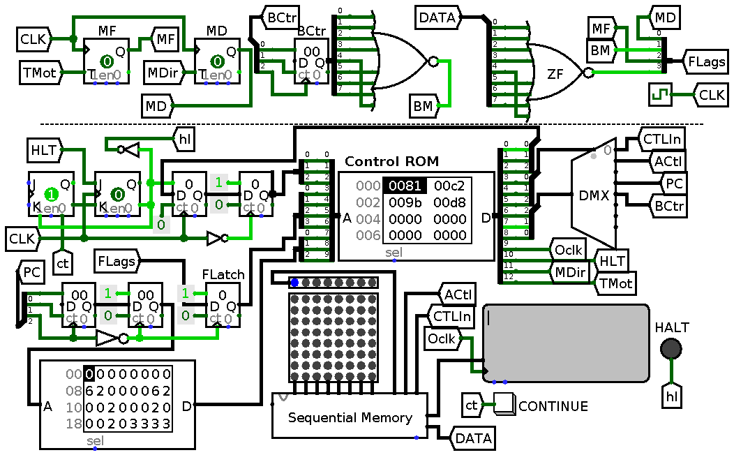
Let us look at schematics. A big DMX
capable to route signals to eight subelements is used to route to just four.
The original logic was to have one route to nowhere to play it extra safe, but
is it really needed? Apparently no, since logical zeroes on control inputs
(which are cared about by the control unit) mean nothing happens to
the counters. So we can easily eliminate one of address lines for counter. To
keep changes minimal let us just remap 010 from ‘no-counter’ to ‘bracket
counter’. The table looses one column: CTRSEL:3 becomes CTRSEL:2. Not
much, but still slightly better than before.
While we are here let us do one more minor update – let us get rid of counters which act as latches. I used them in such way in the first design on purpose: to avoid bringing too many entities into play. Now it is time to replace them with better fitting components – registers. The schematic now looks like this:
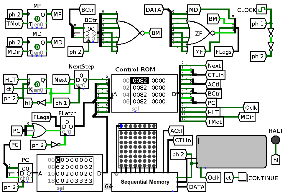
Computer cleanup. DMX is made smaller, counters acting as registers are replaced with actual registers.
Note that additional next step latch turns out to be redundant as well.
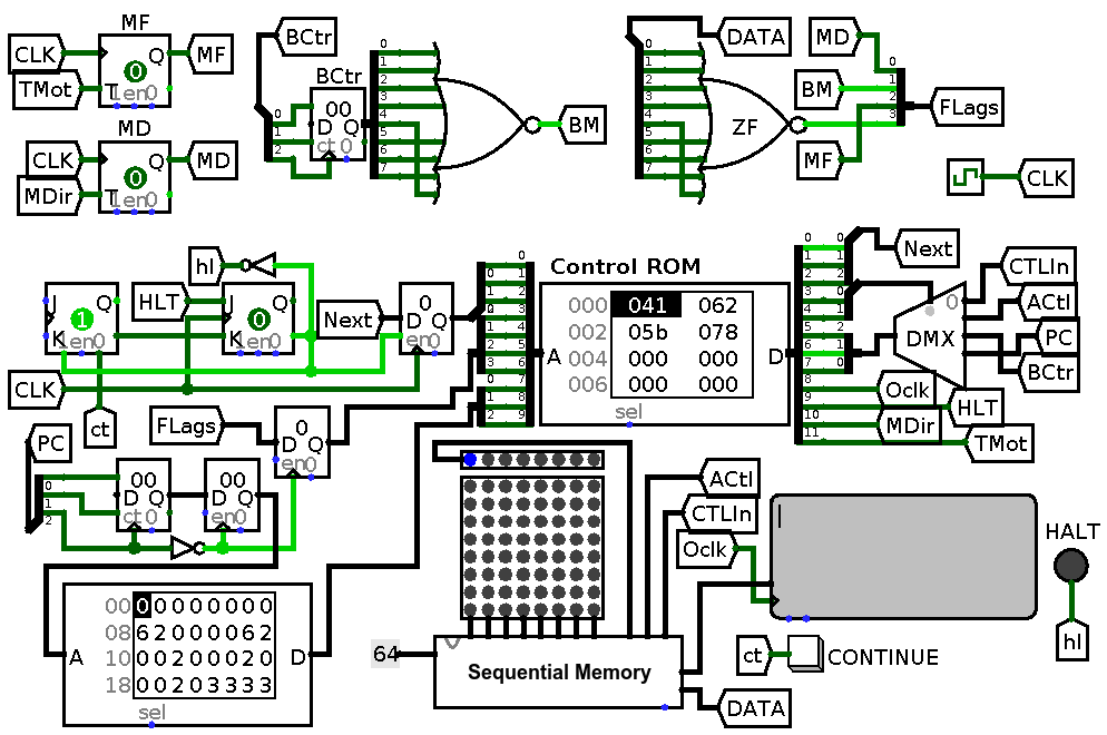
One phase is good, two are better
Let us continue looking closer at the control table. One pattern that keeps popping up everywhere is the use of guardian entries: in order to make sure proper control signals are present on component inputs each step which contains any of counters clock in high state is prepended by exactly the same step but with clock in low state. This is both very visual and very inefficient: if somehow removed it could provide two-fold increase in operation speed.
In fact a hint to a solution to this problem is already present on the schematic. Observe that next instruction propagation is delayed with a separate register. Clock signal for this register is generated by inverting basic clock source which is used to clock next state latch. Thus both rising edge and falling edge of clock signal are used to trigger different substeps within one step. But clock signal used in these circuit is a very low-frequency one, and quite a long time passes between edges. This time is much longer than it is needed for control signals to stabilize1. It would have been nice if a rising edge could be used several times with some delay first to update next step latch and then, when control signals have propagated to counters and stabilized used once again to clock counters. In other words, if clock signal could be split in, say, two with first signal distributed unchanged and the second distributed after been stored somewhere for some period of time, delayed somehow. And that is exactly where propagation delay comes to help us. Recall that it takes time for a signal to traverse any gate. Now consider two inverters placed one after another – they don’t change the signal itself, but introduce a delay two times bigger than delay of a single inverter. Thus in the simplest form clock source could be fed directly to next step latch and simultaneously to a delay line built out of inverters. The output of the delay line would be used as second phase of clock signal.
Unfortunately as of version 2.7.1 Logisim does not provide tools to fully explore the concept of gate delay: apparently it is not available to the end user as a parameter of a gate and it is not quite clear from the documentation to which extent it is accounted for in simulation. Yet it looks like that for the very basic experiments it still works well enough so I will keep using it for now. For less visual, but more in-depth simulation I suggest using other tools, like Qucs which while less visual allow for much more precise control of what is happening in the simulation.
From the perspective of control table the change looks tremendous: almost half of rows disappears! Also CLK data line is not needed any more and can be dropped. The last but not least, now the maximum number of steps in any particular command is not more than four which allows me to remove one address line and one data line for next step. Also I have lost the ability to latch flags only after updating PC because previously I relied on CLK routed to PC for this and now there is no more CLK line. This is not a big deal since all I have to do now is to add an OR gate to detect when PC is getting updated and use its output to enable flags latch update. Note that now output control enables display to react on clock input and auxiliary latch in HLT line goes away.
The resulting circuit is presented below:
Second phase of clock signal is introduced. CLK line is removed from the circuit and control words in control ROM, auxiliary latches are removed, PC update detector is added.
And here is corresponding control table.
To sum up as a result of optimization many components go away (which is pretty good) and control table shrinks in size in two which is very good. But what else could be done?
Further optimization
New control table requires a ROM with 512 words of 10 bits. While the address bus size is important only if one decides to build her own ROM unit – contemporary commercial ones don’t seem to be made for less than 2^13 addresses, data bus width could matter: eight bit are easy to come by, everything above that should be built from two or more ROM units. This looks especially wasteful when one needs ten bits. This makes one wonder if it is possible to shrink control word even more.
Control table entry consists of next step which takes two bits and can’t be shrunk any more – some commands need three steps, two control lines can’t be shrunk as well – all four states are used. Since we have four different counters, CTRSel can’t be shrunk too. Thus six bits are already occupied. Four bits are left for toggling flags and controlling I/O. The good news four bits mean sixteen possible combinations and only five of these possible combinations are actually used, the bad news five states need three bits to represent them:
Num    MDHT
-------------------------------------------------------------------------------
000    0000
001    0001
010    0010
011    1000
100    1100
-------------------------------------------------------------------------------
M - toggle motion flag       D - toggle direction flag
H - halt                     T - enable terminal
Unfortunately every combination must be present and can’t be reduced further, but at least one could easily reduce four last bits to three and use a decoder to produce actual states:
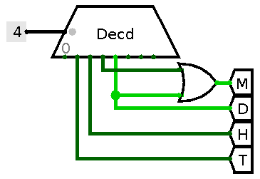
A decoder is used to convert state number to state value.
Unfortunately this still leaves us with nine bits which is one bit more than convenient for a commercially available unit.
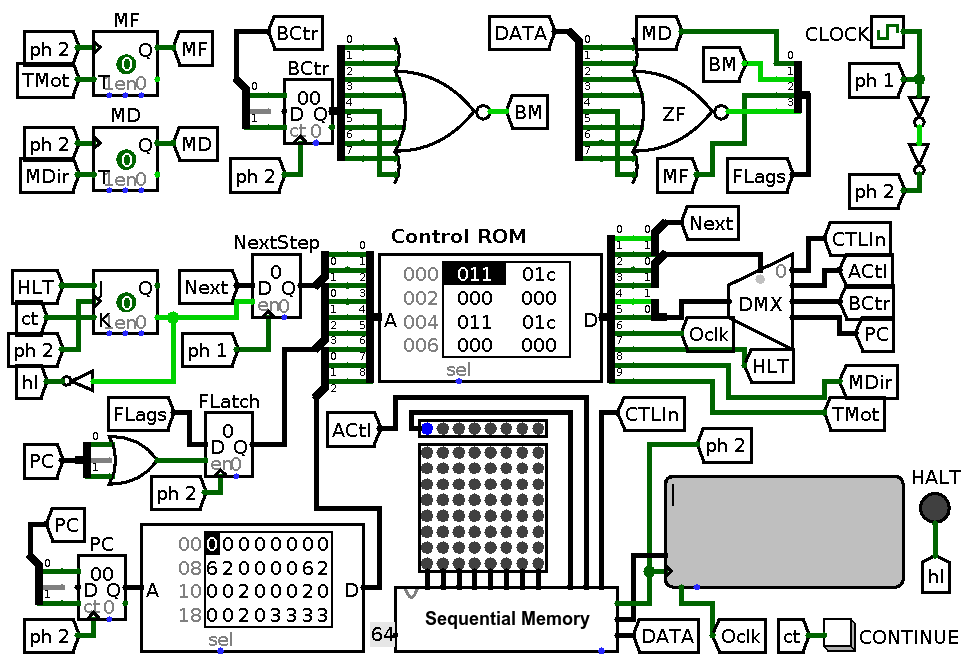
Actually now I am standing at bifurcation point. On one hand I can try harder and shrink control word even more and eventually fit it in eight bits, on the other I can stop tuning control word length and consider instead even bigger speedup. I will act like this: I will start exploring the second option and later will come back to the first one.
Consider this: since counters are independent and all are triggered by phase 2 of clock pulse why update them sequentially when they could be updated simultaneously? This would result in abolition of a demultiplexer and two control lines for counter selection, and introduction of six new control lines which go directly to counters. This way most of the commands will get executed in one step with exception of input command which on one hand introduces huge delays no matter how implemented, on the other is rare and thus does not affect an average program. Now this is a very good speedup for this architecture: it is hard to go below one clock pulse per instruction so I think I’ll settle with it for now, especially given the fact that I started with about four clock cycles per instruction. The resulting schematics looks like this:
A circuit for expanded control word. DMX was removed, next step latch had to stay because input instruction still requires two steps. FLatch has to be clocked with falling edge of phase 2 to avoid thrashing.
Now the control tables becomes compact once again:
              ADDRESS                       STORED VALUE
          +--------------+          +---------------------------+
Command   CODE  ZMBD  STEP             STATE VECTOR     NEXT STEP
-------------------------------------------------------------------------------
 +         000  X0XX   0            0000  01 00 00 01       0
           000  X1X0   0            0000  01 00 00 00       0
           000  X1X1   0            0000  11 00 00 00       0

 -         001  X0XX   0            0000  01 00 00 11       0
           001  X1X0   0            0000  01 00 00 00       0
           001  X1X1   0            0000  11 00 00 00       0

 >         010  X0XX   0            0000  01 00 01 00       0
           010  X1X0   0            0000  01 00 00 00       0
           010  X1X1   0            0000  11 00 00 00       0

 <         011  X0XX   0            0000  01 00 11 00       0
           011  X1X0   0            0000  01 00 00 00       0
           011  X1X1   0            0000  11 00 00 00       0

 .         100  X0XX   0            0001  01 00 00 00       0
           100  X1X0   0            0000  01 00 00 00       0
           100  X1X1   0            0000  11 00 00 00       0

 ,         101  X0XX   0            0010  00 00 00 00       1
           101  X0XX   1            0000  01 00 00 10       0
           101  X1X0   0            0000  01 00 00 00       0
           101  X1X1   0            0000  11 00 00 00       0

 [         110  00XX   0            0000  01 00 00 00       0
           110  10XX   0            1000  01 00 00 00       0
           110  X1X0   0            0000  01 01 00 00       0
           110  X101   0            0000  11 11 00 00       0
           110  X111   0            1100  01 00 00 00       0

 ]         111  00XX   0            1100  11 00 00 00       0
           111  10XX   0            0000  01 00 00 00       0
           111  X1X1   0            0000  11 01 00 00       0
           111  X100   0            0000  01 11 00 00       0
           111  X110   0            1000  01 00 00 00       0
-------------------------------------------------------------------------------
FLAGS = [Zero, Motion, Bracket match, Direction]
STATE VECTOR = [(TOGGLE_MOTION_FLAG, TOGGLE_COUNT_DIRECTION, HLT, TERMCLK),
                (PCL, PCC), (BRAL, BRAC), (ADDRL, ADDRC), (ML, MC)]
Now the computer runs at a decent speed and it is good time to come back to the crossroad and once again try and shrink control word size. And the shrinking would be achieved by utilizing an observation that there are sixteen distinctive control words in the entire table. Think of it. Each word is large, but there are so few of them that they don’t occupy the entire range of which the control bus is capable. Thus we can sacrifice clarity a little and introduce yet another mapping from a four bit number (just enough for the number of states at hand) to control lines state:
Num    State word
-------------------------------------------------------------------------------
0000   0000 01 00 00 00  0
0001   0000 01 00 00 01  0
0010   0000 01 00 00 10  0
0011   0000 01 00 00 11  0
0100   0000 01 00 01 00  0
0101   0000 01 00 11 00  0
0110   0000 01 01 00 00  0
0111   0000 01 11 00 00  0
1000   0000 11 00 00 00  0
1001   0000 11 01 00 00  0
1010   0000 11 11 00 00  0
1011   0001 00 00 00 00  1
1100   0010 00 00 00 00  1
1101   1000 01 00 00 00  0
1110   1100 01 00 00 00  0
1111   1100 11 00 00 00  0
-------------------------------------------------------------------------------
STATE VECTOR = [(TOGGLE_MOTION_FLAG, TOGGLE_COUNT_DIRECTION, HLT, TERMCLK),
                (PCL, PCC), (BRAL, BRAC), (ADDRL, ADDRC), (ML, MC), NEXT_STEP]
Then this mapping could be used to populate control table, output of which is fed to a device which contains the mapping above. It could be either conventional ROM as I used in the circuit for the demonstration purpose, or a device similar to the decoder described above. This allows us to both avoid the use of extra components in control units and still have all the benefits of wide control words.
Final circuit looks like this:
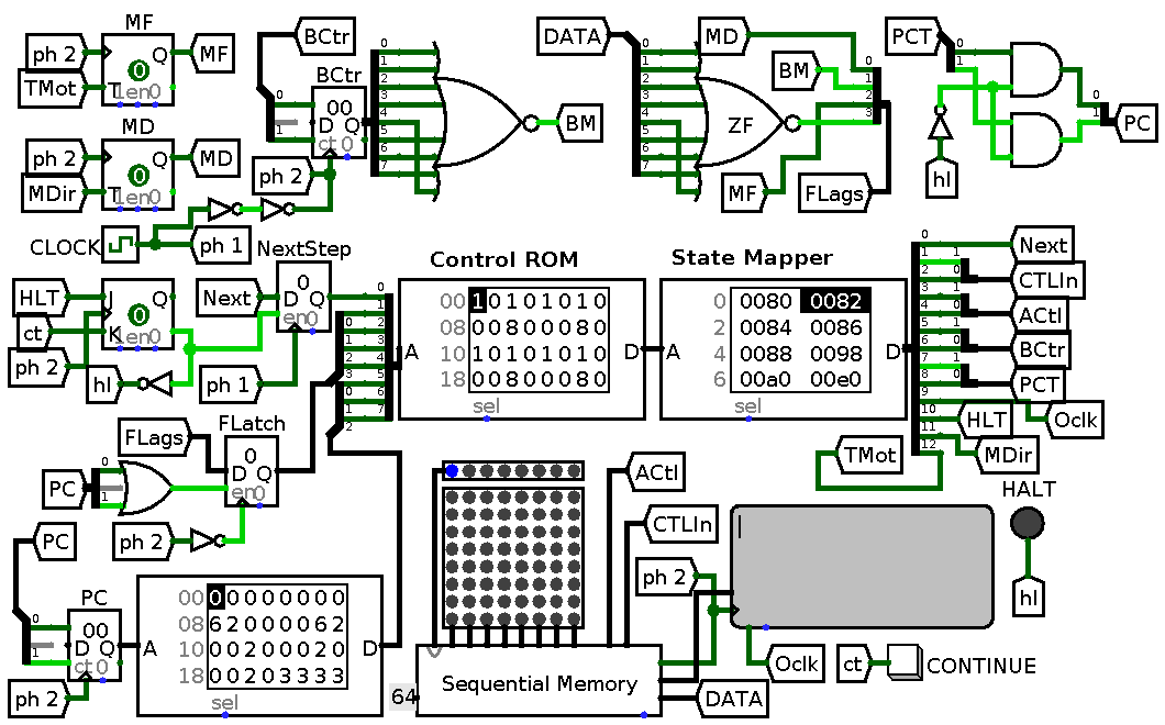
A final circuit which utilizes both wide control words and compact storage. Wide control words are stored in separate device with just four address bits.
Control table for it could be easily derived from expanded control table and substitution table. Circuits for this post could be found in a usual place
Afterword
This post has finalized the basics of development of BrainF–k computer: the design is relatively performant and at the same time still easy to understand. This design is ready to be translated to be implemented in hardware yet to do that I have to deal with some debt first, namely I have to discuss various ways to implement memory units and displays. After that everything will be ready to build a real BrainF–k computer.
-
Signals don’t need to be stabilized in Logisim, but here I am referring to what happens in a real circuit. ↩